by Gayle Towell
I am proud to share that my recent APEX EXPO technical paper, “Rethinking Area Ratio: A Physics-Based Model for Predicting Solder Paste Transfer Efficiency for Thin Stencils,” received the NextGen Best Paper Award. I am furthermore grateful to AIM for giving me the support, encouragement, and room to pursue the kind of technical questions that led to this work.

Bringing a Physics Background to Solder
This award recognizes the top paper from next-generation industry technologists with less than five years of experience. Many are surprised to learn this, but I have only been in this industry for three years. That said, I did not exactly arrive straight out of school.
I have a background in math and physics and have spent years teaching undergraduates and running physics labs before transitioning to technical writing and then pivoting to my role at AIM. I must say, I’ve found a happy home in the land of solder for electronics manufacturing. After all, it’s full of fundamental science: mechanics, fluid dynamics, thermodynamics, materials behavior, and more. It is also full of real-world production variables that make those fundamentals complicated, interesting, and useful.
This paper grew out of that intersection between first principles and practical manufacturing: a familiar printing challenge, a question I could not stop thinking about, and a closer look at the physics behind it.
An Observation in Need of Explanation
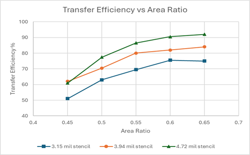
In ultrafine printing applications, many have noticed that thin stencils seem to require larger area ratio limits than conventional guidance would suggest. The familiar 0.60 threshold is not enough. Especially when getting down to 1-2 mil stencil thickness, a higher value is needed for reliable paste transfer.
This is useful to know, but it bothered me that I could not fully explain dlaczego.
My instinct was to go back to the foundation of the area ratio model itself. Area ratio is derived from a force balance: the force pulling the solder paste onto the board versus the force holding it inside the stencil aperture. Traditionally, that model considers adhesion between the paste and the board, and adhesion between the paste and the stencil walls. But when I looked at the force diagram, something was missing.
The force of gravity.
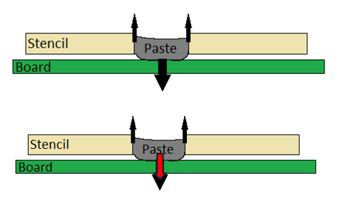
Gravity!
Gravity may seem like a small factor in stencil printing, but a quick thought experiment puts things in perspective: suppose you did the printing process upside down. Would you expect the same results? No. Why? Because of gravity.
When all stencils were of similar thickness, this was easy to overlook. However, adhesive forces scale with surface area. Gravitational force scales with volume. So, when stencils start getting thinner, a discrepancy emerges. And once gravity is included in the model, the discrepancy begins to make sense: thinner stencils require higher area ratios because there is less gravitational assistance helping the paste release.
A New Model Emerges
From there, I developed a modified force relationship that incorporates gravitational force into the traditional area ratio model. The result is a stencil-thickness-dependent area ratio limit, rather than a single one-size-fits-all threshold. In the paper, I applied the model to existing published data and found that it was consistent with observed transfer efficiency trends across different stencil thicknesses, paste types, aperture designs, and stencil coatings.
That part was especially exciting. This was not just an interesting theoretical exercise. It explained something practitioners had already observed, and it provided a framework that could eventually support more precise stencil design guidance for ultrafine solder paste printing.
From Curiosity to Practical Guidance
That this work won an award was a meaningful recognition of its potential value to the industry. More than anything, though, I see this paper as a reminder that even familiar manufacturing challenges can benefit from a fresh look at the underlying science.
Solder paste printing is not new. Area ratio is not new. But by asking a basic physics question and following it carefully, we can still find opportunities to improve understanding, refine best practices, and contribute something useful to the industry.
I am grateful to work for a company that supports technical curiosity and gives me room to stretch my wings. For me, this project is a clear example of how fundamental science, practical manufacturing experience, and a little intellectual freedom can come together to create something useful.
Referencje
Härter, S., Niemann, J., Franke, J., Schake, J., & Whitmore, M. (2016). The effect of area shape and area ratio on solder paste printing performance. Proceedings of SMTA International, September 25–29, 2016, Rosemont, IL, USA.