By Gayle Towell
I recently attended the 75th annual Electronic Components and Technology Conference (ECTC) at the end of May. The conference brought together a record number of attendees and technical presentations. It also highlighted the rapid evolution of chip-scale packaging in the AI era.
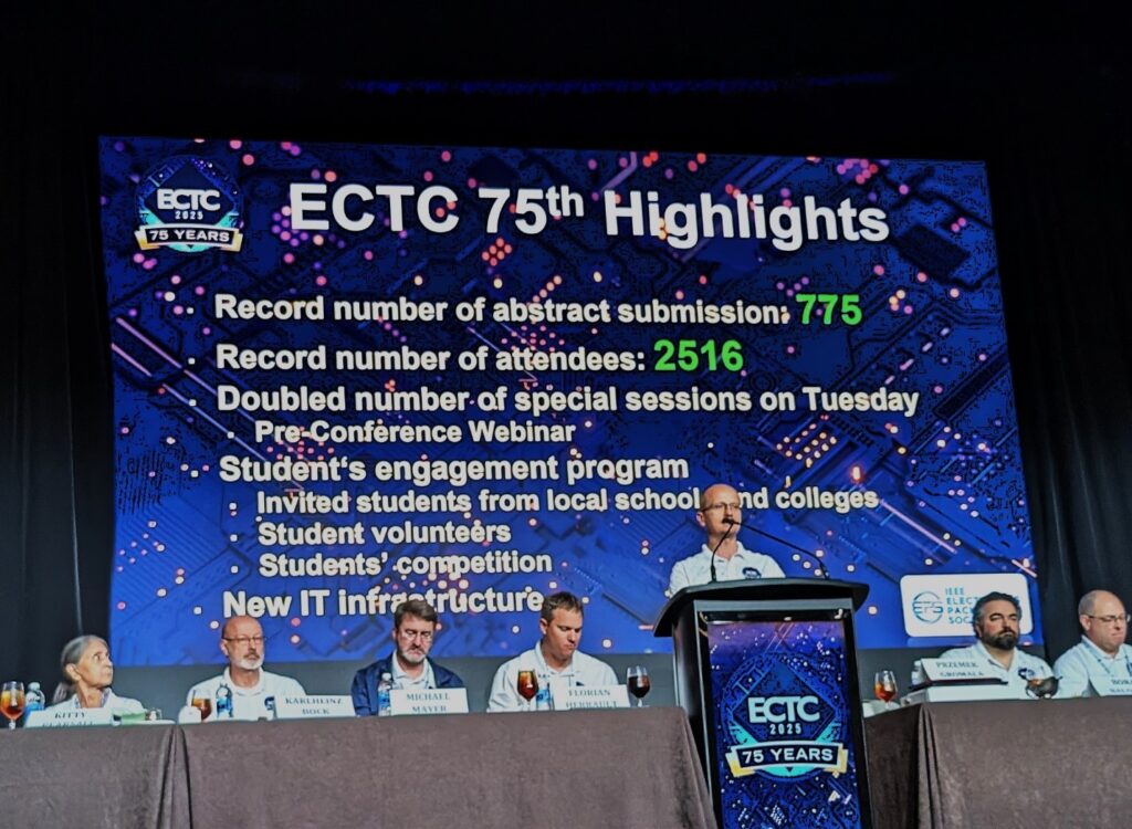
With more than 2,500 participants and nearly 800 technical submissions, the event offered an exceptional opportunity to explore the current state—and future trajectory—of semiconductor packaging and interconnect technologies. For AIM, attending ECTC was a chance to further explore the role of solder this landscape. It provided insights into how our materials must evolve to meet tomorrow’s demands.
Advanced Packaging
The rapid pace of innovation, particularly around AI applications, is reshaping chip architectures. Multilayer designs—including 2.5D and 3D package stacking—are becoming common. This introduces new assembly challenges and expands the range of materials and processes needed to support reliable interconnects.
Solder still plays a key role in these packages, primarily in bumps, BGAs, and sometimes as preforms. While direct copper-to-copper bonding is gaining ground, solder continues to offer performance and manufacturing advantages. This is especially true in scenarios where reworkability, process control, and material compatibility are essential.
Key Trends and Takeaways From ECTC 2025
AI is Driving Everything
As demands for computing power skyrocket, AI-capable chips must push the limits of thermal management and interconnect density. The three pillars are clear: power in, heat out, and loss reduction across the signal path.
Chip Warpage is a Growing Concern
CPUs and GPUs are increasing in size to handle AI workloads. This means managing warpage during reflow is more important than ever. Recent data suggests that low-temperature solders—particularly in BGA spheres—can mitigate this warpage even when reflowed at standard SAC temperatures.
Ultrafine Solder Pastes Are Essential
When it comes to solder paste printing, ultrafine particle sizes—such as Type 6 or Type 7—are needed. These are required to meet the precision and volume control demands of advanced packaging. AIM currently offers these ultrafine solder pastes to support customers working at the leading edge of miniaturization.
Thermal Interface Materials (TIMs)
There is enormous focus on TIM development, including TIM1.5 and TIM2.0. Engineers are seeking better ways to manage heat across stacked packages and dense assemblies.
Low Temperature Soldering Gaining Momentum
In contrast to the SMT space, where LTS adoption has been slow, chip-scale applications are embracing these alloys. This presents opportunities for alloy development and reflow process optimization.
Fluxless Soldering Technologies
Fluxless methods—like formic acid reflow and plasma oxide removal—were widely discussed. As demand for residue-free processes grows (especially in low-standoff or high-density assemblies), it’s worth watching whether these technologies make their way into SMT.
Laser Reflow for Solder Attach
Many studies presented at ECTC explored the benefits of laser reflow for bumps and solder paste. They cited reduced IMC formation, refined microstructures, and lower thermal exposure for sensitive components.
Underfill and Side Fill Materials
Protective encapsulants—especially those used with stacked chips or high-power modules—remain critical to long-term reliability in harsh use conditions.
What Comes Next
This conference was not only informative—it was energizing. The insights gained are helping shape AIM’s strategic direction as we evaluate new materials, markets, and collaborations.
We are actively reviewing the solder-related papers from ECTC and combining these findings with our ongoing research into advanced packaging. Cross-functional conversations between R&D, product management, and leadership are underway to determine which trends and technologies warrant deeper exploration.
Keeping a close eye on everything from fluxless soldering processes to low-temperature metallurgy helps us develop future-ready solutions for our customers.
As advanced packaging grows in complexity and importance, AIM is committed to delivering solder materials and technical expertise to support high-performance electronics at every scale.