


Par Gayle Towell
Le rapport de surface (AR) est depuis longtemps la norme industrielle pour prédire l'efficacité de transfert de la pâte à braser (TE) et guider la conception de l'ouverture du pochoir. Toutefois, à mesure que la fabrication électronique s'oriente vers des pas ultrafins et des pochoirs plus minces, des incohérences sont apparues dans le TE, bien que les valeurs AR soient supérieures au seuil recommandé de 0,60. Cette étude examine les fondements théoriques de la libération de la pâte du pochoir, en se concentrant sur l'interaction entre les forces gravitationnelles (qui augmentent avec le volume de la pâte) et les forces d'adhésion entre la pâte, les parois du pochoir et le substrat (qui augmentent avec la surface).
Nous proposons ici un modèle alternatif pour les limites AR variables qui tient compte des variations de l'épaisseur du pochoir. Pour tester cette approche, le modèle a été appliqué à des données expérimentales préexistantes obtenues à partir d'articles précédemment publiés dans lesquels des tests d'impression avec différentes épaisseurs de pochoir ont été utilisés. Les résultats indiquent qu'une limite AR dépendant de l'épaisseur du pochoir fournit un prédicteur plus précis de la TE pour différentes conceptions de pochoirs et pourrait informer les futures normes industrielles pour l'impression de pâte à braser ultrafine.
Introduction
Le rapport de surface est largement utilisé dans la technologie de montage en surface (SMT) comme indicateur permettant de prédire l'efficacité du transfert de la pâte à souder lors de l'impression au pochoir. Défini comme le rapport entre la section transversale de l’ouverture et la surface totale des parois de celle-ci, ce rapport permet d’évaluer si la pâte à souder se détachera efficacement du pochoir pour se déposer sur le circuit imprimé (PCB).
Les recommandations du secteur, telles que la norme IPC-7525 [1], préconisent généralement un rapport de surface minimal de 0,60 pour obtenir de bonnes performances d’impression. Cependant, à mesure que les composants électroniques continuent de rapetisser et que l’épaisseur des pochoirs diminue pour s’adapter à des pas plus fins, cet indicateur commence à montrer ses limites. Les utilisateurs constatent fréquemment que le seuil de 0,60 ne s’applique pas de manière universelle, en particulier lorsque la géométrie des ouvertures ou les matériaux des pochoirs s’écartent des normes conventionnelles. Ces divergences suggèrent que la formulation initiale de la règle du rapport de surface repose sur des hypothèses simplificatrices qui ne sont peut-être plus valables dans les conditions de fabrication actuelles.
Le rapport de surface comme indicateur de l'efficacité du transfert d'impression
Le seuil de rapport de surface actuellement utilisé repose sur un modèle d’équilibre des forces impliquant deux forces d’adhérence : l’adhérence entre la pâte à souder et les parois du pochoir, et l’adhérence entre la pâte à souder et le substrat. L’hypothèse est que le détachement de la pâte s’effectue avec succès lorsque la force d’adhérence qui attire la pâte vers la carte dépasse la force d’adhérence qui la retient à l’intérieur de l’ouverture. Dans ce modèle, la force d’adhérence entre la pâte à souder et toute surface est considérée comme proportionnelle à la surface de contact et à l’adhérence intrinsèque par unité de surface. Cela conduit à la condition suivante pour un détachement réussi de la pâte : C₁A₁ > C₂A₂,
où :
- C₁ correspond à la force d'adhérence par unité de surface entre la pâte à souder et le circuit imprimé
- A₁ correspond à la section transversale de l'ouverture
- C₂ correspond à la force d'adhérence par unité de surface entre la pâte à souder et les parois du pochoir
- A₂ correspond à la surface totale de la paroi du pochoir en contact avec la pâte
En réorganisant cette relation, on obtient l'inégalité du rapport des aires :
Rapport des aires = A₁ / A₂ > C₂ / C₁
Les constantes C₁ et C₂ étant difficiles à mesurer directement — chacune dépendant des propriétés du matériau, de l'état de surface et des conditions environnementales —, le seuil de 0,60, qui fait référence dans le secteur, a été établi de manière empirique.
Ce rapport donne des résultats satisfaisants dans de nombreux cas de figure courants en matière d'impression. Cela dit, des écarts peuvent tout de même se produire. Par exemple, les pochoirs couchés — dont les parois sont plus lisses — peuvent réduire la valeur C₂, permettant ainsi un décollement satisfaisant avec des rapports de surface plus faibles. À l'inverse, les cas impliquant des pâtes exceptionnellement collantes ou des parois de pochoir rugueuses peuvent nécessiter des rapports de surface plus élevés pour garantir un décollement fiable.
De plus, ce modèle ne tient pas compte de tous les facteurs physiques influençant le décollement de la pâte. La cohésion interne d’une pâte, par exemple, peut être plus faible que son adhérence au pochoir, ce qui complique encore davantage la dynamique du transfert. Ces limites indiquent que, bien que la règle actuelle du rapport de surface constitue une ligne directrice utile, elle n’est en fin de compte qu’une représentation trop simplifiée d’un processus physique plus complexe.
Limites du rapport de surface lorsque l'épaisseur du pochoir est réduite
On considère généralement que l'utilisation d'un pochoir plus fin améliore l'efficacité du transfert de la pâte à souder. Cette idée repose souvent sur des cas de figure où, pour conserver le même volume de dépôt ou la même empreinte, la réduction de l'épaisseur du pochoir nécessite d'augmenter le rapport de surface, ce qui se traduit par une amélioration des performances de transfert, conformément au modèle classique.
Cependant, lorsque le rapport de surface est maintenu constant pour différentes épaisseurs de pochoir — ce qui signifie que les dimensions de l'ouverture sont ajustées proportionnellement —, de nombreux professionnels ont observé l'effet inverse : les pochoirs plus fins ont tendance à offrir un rendement de transfert plus faible, et non plus élevé. Ce phénomène a été rapporté de manière anecdotique dans divers environnements de production, mais jusqu’à présent, aucun travail publié n’a fourni d’explication théorique ni de modèle quantitatif permettant de le rendre compte.
Cet article propose un modèle révisé basé sur les forces, fondé sur les principes fondamentaux de la physique. Ce modèle intègre un facteur supplémentaire – l'influence de la gravité sur le dépôt de pâte à souder – dans l'équation classique de libération et établit une nouvelle relation fonctionnelle entre le rapport de surface et l'épaisseur du pochoir.
Cette approche fournit une base théorique expliquant la diminution observée de l'efficacité de transfert lorsque les pochoirs sont plus fins et permet d'estimer les limites minimales du rapport de surface adaptées à des géométries de pochoirs spécifiques.
Réexamen du modèle des forces : une nouvelle proposition
Pour expliquer la baisse observée du rendement de transfert lorsque l'épaisseur du pochoir est réduite à rapport de surface constant, il est nécessaire de réexaminer les hypothèses sous-jacentes concernant les forces en jeu. Le modèle classique ne prend en compte que deux forces dans le processus de décollement : l’adhérence entre la pâte et les parois du pochoir, et l’adhérence entre la pâte et le substrat. Cependant, cette simplification néglige un troisième facteur important : la force de gravité agissant sur le volume de pâte à souder.
La force gravitationnelle est proportionnelle au volume du dépôt de pâte, tandis que la force d'adhérence entre la pâte et la carte est proportionnelle à la surface. La surface et le volume n'étant pas proportionnels de manière linéaire l'un par rapport à l'autre, cela entraîne un décalage qui s'accentue avec des pochoirs plus fins et des dépôts plus petits. En d’autres termes, à mesure que le pochoir s’amincit, la masse — et donc l’aide gravitationnelle à la libération de la pâte — diminue plus rapidement que la force d’adhérence à la carte, ce qui perturbe le comportement de libération attendu. Ce décalage n’est pas pris en compte dans le modèle traditionnel du rapport de surface.
Adhérence et frottement dans l'interaction entre le pochoir et la paroi
Lors de l'élaboration du modèle révisé, il a fallu déterminer si l'interaction entre la pâte et les parois du pochoir devait être considérée strictement comme une adhérence ou comme une forme de frottement de glissement. Si le frottement est le mécanisme dominant, la force de résistance serait décrite par : F = μN, où μ est le coefficient de frottement et N la force normale.
Il convient de noter que la force normale exercée par la pâte sur les parois du pochoir dépend de la pression, qui varie en fonction de la profondeur, x, selon la relation pression = . La force totale exercée sur les parois sous l'effet de la pression s'obtient en intégrant la pression sur la surface des parois. Dans ce cas, la force exercée sur les parois s'écrit :
F = = μρgPT²/2, ce qui peut s'écrire sous la forme μρgA₂T/2.
Où :
- ρ est la densité de la pâte
- g est l'accélération gravitationnelle
- P correspond au périmètre de l'ouverture
- T correspond à l'épaisseur du pochoir
- A₂ correspond à la surface de la paroi du pochoir
Cependant, des données d’observation — telles que les analyses de vidéos à haute vitesse réalisées par Chrys Shea [2] — suggèrent que la libération de la pâte se produit principalement par étirement et détachement cohésifs plutôt que par glissement le long des parois. Dans ce modèle, l’interaction entre le pochoir et la paroi est donc traitée comme une force d’adhérence pure : C₂A₂, où C₂ est la force d’adhérence par unité de surface. Dans le cadre de travaux futurs, cette hypothèse pourrait être réexaminée pour des scénarios spécifiques, tels que des pochoirs hautement polis ou revêtus, ou des pâtes à souder à faible cohésion. Pour l’instant, le modèle part du principe que l’adhérence est le facteur dominant.
Relation de force modifiée pour la libération de la pâte
En intégrant la force gravitationnelle dans la condition initiale de libération, on obtient un équilibre des forces révisé : C₁A₁ + ρVg > C₂A₂
Où :
- C₁ et C₂ correspondent respectivement à la force d'adhérence par unité de surface entre la pâte et le carton, et entre la pâte et le support.
- A₁ et A₂ correspondent respectivement à la section transversale de l'ouverture et à la surface des parois du pochoir
- ρ est la densité de la pâte
- V est le volume du dépôt de soudure
- g est l'accélération gravitationnelle
Puisque V = A₁T, où T est l'épaisseur du pochoir, et afin de regrouper les constantes pour plus de clarté, posons C₃ = ρg, soit la force gravitationnelle par unité de volume. En substituant ces valeurs, on obtient : C₁A₁ + C₃A₁T > C₂A₂
En factorisant A₁, on obtient : Rapport des aires = A₁ / A₂ > C₂ / (C₁ + C₃T)
Cette expression décrit la limite du rapport de surface nécessaire pour garantir un décollement correct de la pâte, en fonction de l'épaisseur du pochoir. Il est important de noter qu'elle montre que, lorsque T diminue, le dénominateur diminue également, ce qui augmente le rapport de surface requis.
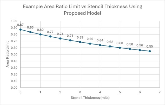
Pour simplifier davantage l'expression, posons a = C₂ / C₃ et b = C₁ / C₃. La limite du rapport de surface devient alors : Limite du rapport de surface = Y(T) = a / (b + T)
À titre d'exemple illustrant cette relation, supposons qu'une limite de rapport de surface de 0,60 s'applique à un pochoir de 5 mils (127 µm) et passe à 0,80 pour un pochoir de 1 mil (25 µm). Ces valeurs correspondent à a = 9,6 et b = 11. La courbe qui en résulte, illustrée à la figure 1, montre comment les limites du rapport de surface varieraient en fonction de l'épaisseur du pochoir, sur la base de ces conditions aux limites.
Validation du modèle proposé à l'aide de données existantes
Afin d'évaluer la validité du modèle de rapport de surface proposé, plusieurs études publiées ont été examinées, qui rendaient compte de l'efficacité du transfert d'impression pour différentes épaisseurs de pochoir et différents rapports de surface. Bien qu'aucune étude visant directement à quantifier les limites du rapport de surface en fonction de l'épaisseur du pochoir n'ait été identifiée, plusieurs d'entre elles fournissaient des ensembles de données adaptés à une analyse rétrospective.
Ces données permettent de déterminer si les limites du rapport de surface nécessaires pour atteindre une efficacité de transfert de 75% augmentent à mesure que l'épaisseur du pochoir diminue, comme le prévoit le modèle. Pour chaque ensemble de données, on a représenté graphiquement l’efficacité de transfert en fonction du rapport de surface, on a déterminé les seuils de rapport de surface correspondant à l’efficacité 75%, et on a ajusté les points obtenus à la fonction proposée afin d’en évaluer la cohérence.
Validation à l'aide d'ensembles de données comportant trois épaisseurs de pochoir
Le premier ensemble de données provient de l'article intitulé “ Étude sur l'utilisation de pochoirs à revêtement nanométrique pour améliorer l'impression de pâte à souder avec de faibles rapports de surface d'ouverture des pochoirs ” [3]. Cette étude a présenté des résultats d’efficacité de transfert pour des épaisseurs de pochoir de 3, 4 et 5 mils, sur trois types de pâte à souder (type 3, type 4 et type 5), et comprenait à la fois des conditions avec des pochoirs non revêtus et des pochoirs nanorevêtus. L’objectif initial de l’étude était d’évaluer les avantages des nano-revêtements ; cependant, la structure des données s’est avérée particulièrement adaptée pour tester la capacité prédictive du modèle de rapport de surface proposé.
Les résultats obtenus pour les pochoirs non enduits et enduits, pour chaque type de pâte et chaque épaisseur de pochoir, ont été analysés séparément. Pour chaque combinaison, le rendement de transfert a été représenté graphiquement en fonction du rapport de surface. Ces résultats sont présentés à la figure 2.
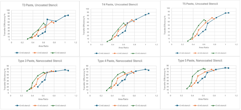
Ces données montrent clairement que les pochoirs plus fins présentent systématiquement des rendements de transfert inférieurs pour des rapports de surface équivalents. Cette tendance correspond parfaitement aux prévisions du modèle proposé.
Afin de garantir la cohérence et la comparabilité de l'ensemble de données, l'accent a été mis sur un sous-ensemble spécifique des données disponibles : les résultats de transfert d'impression pour les pastilles de composant 01005. Ce type d'ouverture était systématiquement présent pour tous les types de pâte, toutes les épaisseurs de pochoir et toutes les conditions de revêtement, ce qui en faisait un candidat idéal pour la validation du modèle.
Pour chaque type de pâte et chaque condition de pochoir, un ajustement linéaire a été appliqué au graphique correspondant représentant le rapport entre l'efficacité de transfert et le rapport de surface. À partir de chaque courbe ajustée, la valeur du rapport de surface nécessaire pour atteindre une efficacité de transfert de 75% a été interpolée. Les valeurs seuils de rapport de surface ainsi obtenues pour toutes les combinaisons de type de pâte, d'épaisseur de pochoir et d'état de revêtement sont résumées dans le tableau 1.
Tableau 1. Seuils des rapports de surface issus des ajustements graphiques.
| Pochoir non enduit | Pochoir à revêtement nanotechnologique | ||||||||||
| T3 | T4 | T5 | T3 | T4 | T5 | ||||||
| Épaisseur du pochoir | Seuil de l'AR | Épaisseur du pochoir | Seuil de l'AR | Épaisseur du pochoir | Seuil de l'AR | Épaisseur du pochoir | Seuil de l'AR | Épaisseur du pochoir | Seuil de l'AR | Épaisseur du pochoir | Seuil de l'AR |
| 3 | 0.953 | 3 | 0.906 | 3 | 0.878 | 3 | 0.930 | 3 | 0.919 | 3 | 0.822 |
| 4 | 0.875 | 4 | 0.810 | 4 | 0.766 | 4 | 0.753 | 4 | 0.783 | 4 | 0.714 |
| 5 | 0.707 | 5 | 0.692 | 5 | 0.636 | 5 | 0.625 | 5 | 0.618 | 5 | 0.546 |
Il convient de noter que la réduction de la taille des particules de pâte semble également entraîner une diminution des valeurs seuils du rapport de surface dans l’ensemble de ces séries de données, à une seule exception près : la pâte de type 4 imprimée à l’aide d’un pochoir nanorevêtu de 4 mils. Cette anomalie est probablement due à une incertitude ou à une erreur de mesure. Cet effet pourrait faire l'objet d'une étude future visant à évaluer l'impact de la taille des particules de pâte sur ce modèle.
Les données du tableau 1 ont ensuite été utilisées pour évaluer la précision prédictive du modèle proposé, défini comme suit : Y(T) = a / (b + T). Une analyse de régression non linéaire a été réalisée pour chaque série de données afin de déterminer les paramètres a et b offrant le meilleur ajustement, et la qualité de chaque ajustement a été évaluée à l’aide du coefficient de détermination (R²). Les ajustements obtenus sont illustrés dans les figures 3, et les valeurs des paramètres ainsi que les mesures R² correspondantes sont résumées dans le tableau 2.
Tableau 2. Paramètres d'ajustement.
| Non revêtu, T3 | Non revêtu, T4 | Non revêtu, T5 | Nanorevêtement, T3 | Nanorevêtement, T4 | Nanorevêtement, T5 | |
| a | 6.046 | 6.109 | 4.848 | 3.847 | 4.067 | 3.627 |
| b | 3.246 | 3.697 | 2.481 | 1.132 | 1.382 | 1.352 |
| R2 | 0.919 | 0.982 | 0.983 | 0.999 | 0.974 | 0.946 |
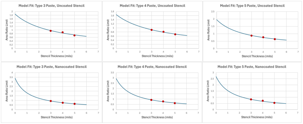
Bien que chaque ajustement soit limité par le nombre restreint de points de données — qui reflète les trois épaisseurs de pochoir évaluées —, les résultats montrent une forte cohérence avec le modèle proposé, et les ajustements sont jugés raisonnables dans ces limites.
Un deuxième article a été sélectionné afin d’évaluer plus en détail le modèle proposé à l’aide d’un protocole expérimental différent. Intitulé “ The Effect of Area Shape and Area Ratio on Solder Paste Printing Performance ” [4], cet article examine comment la forme de l’ouverture et le rapport de surface influencent l’efficacité du transfert lors de l’impression. Il convient de noter que cette étude inclut des données relatives à plusieurs géométries d’ouverture imprimées sur trois épaisseurs de pochoir différentes — 80 µm (3,15 mils), 100 µm (3,94 mils) et 120 µm (4,72 mils) — à l’aide d’un seul type de pâte.
Par souci de cohérence avec les analyses précédentes, les données relatives aux ouvertures de forme carrée ont été isolées, ce qui a permis une comparaison directe de l’efficacité de transfert d’impression pour différentes épaisseurs de pochoir, à des rapports de surface identiques. Cette uniformité élimine la variabilité due à la géométrie des ouvertures et rend l’ensemble de données particulièrement bien adapté pour évaluer si l’épaisseur du pochoir, à elle seule, influence l’efficacité de transfert. La figure 4 présente le graphique résultant de l'efficacité de transfert en fonction du rapport de surface pour les trois épaisseurs de pochoir.
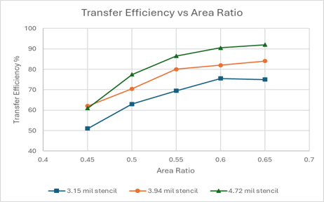
Comme pour l’ensemble de données précédent, le pochoir plus fin présente systématiquement un rendement de transfert inférieur pour des rapports de surface identiques, ce qui confirme la prédiction principale du modèle selon laquelle une épaisseur de pochoir réduite augmente le rapport de surface minimal requis pour un transfert acceptable. Des ajustements linéaires ont été effectués sur chaque ensemble de données relatif à l’épaisseur des pochoirs, et le rapport de surface correspondant à une efficacité de transfert de 75% a été interpolé. Ces valeurs seuils sont résumées dans le tableau 3.
Tableau 3. Seuils des rapports de surface issus des ajustements graphiques.
| Épaisseur du pochoir (mils) | Seuil du rapport de surface |
| 3.15 | 0.62 |
| 3.94 | 0.54 |
| 4.72 | 0.51 |
À partir de ces données, les résultats ont de nouveau été ajustés au modèle proposé, Y(T) = a / (b + T). Les paramètres d'ajustement optimal étaient les suivants : a = 4,306, b = 3,853, R² = 0,962 ; la courbe du modèle correspondante est représentée sur la figure 5.
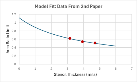
Bien qu’il se limite à trois épaisseurs de pochoir, la cohérence de cet ensemble de données — combinée à la tendance observée et à la qualité de l’ajustement — vient renforcer la validité du modèle proposé. La valeur élevée du R² indique que la forme fonctionnelle rend bien compte de l’effet de l’épaisseur du pochoir, même en présence de facteurs de confusion potentiels tels que la variabilité de la pâte ou les effets de nivellement à des épaisseurs plus élevées.
Validation à l'aide d'ensembles de données comportant deux épaisseurs de pochoir
Afin d'évaluer plus en détail la pertinence du modèle proposé, plusieurs études supplémentaires présentant des résultats sur l'efficacité du transfert pour deux épaisseurs de pochoir ont été analysées. Bien que ces études fournissent moins de points de données, elles permettent de mieux déterminer si la relation entre l'épaisseur du pochoir et le rapport de surface requis pour un transfert efficace reste valable avec différents matériaux, procédés et conditions d'impression.
Les données ont été extraites des articles intitulés “ Étude fondamentale sur un procédé d’impression sécurisé utilisant des pochoirs Nanowork pour les composants 01005 ” [5] et “ Effet de la technologie des pochoirs sur l’impression à pas ultra-fin ” [6]. Le premier de ces articles présentait des données sur le rendement de transfert pour des pochoirs d’une épaisseur de 80 µm et 100 µm, évaluées à la fois avec des pâtes à souder de type 4 et de type 5. Par souci de cohérence, l’accent a été mis sur les résultats associés aux ouvertures rectangulaires arrondies. Le deuxième article comparait plusieurs types de pochoirs, notamment des pochoirs découpés au laser et électroformés, avec et sans nano-revêtements. Les données ont été recueillies pour des épaisseurs de pochoir de 100 µm et 120 µm. Bien que les données incluent divers types d’ouvertures, plusieurs scénarios présentant des formes d’ouvertures similaires ont été identifiés afin de permettre une comparaison directe. Les graphiques représentant l’efficacité de transfert en fonction du rapport de surface, établis à partir des données de ces articles, figurent à la figure 6.
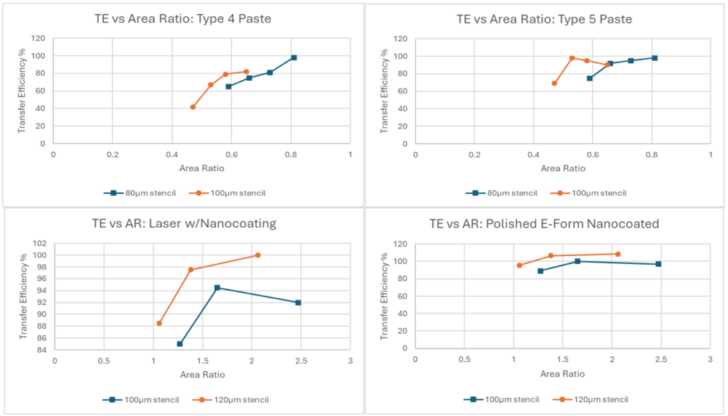
Bien que ces études se limitent chacune à deux épaisseurs de pochoir, la tendance constante observée dans l'ensemble des jeux de données corrobore le principe fondamental du modèle proposé. Dans chaque cas, la diminution de l'épaisseur du pochoir entraîne une baisse mesurable de l'efficacité de transfert à rapport de surface constant — un effet que le seuil de rapport de surface conventionnel ne parvient pas à expliquer, mais qui est prévu par la formulation révisée fondée sur la physique.
Synthèse des résultats et perspectives futures
Le modèle proposé, qui introduit un terme dépendant de l’épaisseur dans la formulation traditionnelle du rapport de surface, présente une forte concordance avec un large éventail de données expérimentales existantes. Plusieurs études ont montré que l'épaisseur du pochoir influençait de manière significative l'efficacité du transfert de la pâte à souder, même lorsque le rapport de surface était maintenu constant — une tendance que la norme IPC-7525 ne parvient pas à expliquer. En revanche, le modèle révisé rend compte avec précision de ce comportement grâce à une relation simple, fondée sur la physique, qui intègre la force gravitationnelle et le volume de pâte.
Bien que la validation actuelle se limite à des ensembles de données comportant deux ou trois épaisseurs de pochoir, la cohérence de la tendance observée d’une étude à l’autre — quels que soient le type de pâte, la forme de l’ouverture ou le revêtement du pochoir — apporte un premier soutien convaincant à la capacité prédictive du modèle.
Afin de renforcer et d'affiner davantage ce modèle, les travaux futurs comprendront une étude contrôlée évaluant les performances d'impression pour cinq épaisseurs de pochoir ou plus, en maintenant constants le rapport de surface, le type de pochoir et son revêtement, ainsi que le type de pâte à souder. Cela permettra un ajustement plus rigoureux du modèle et offrira une meilleure résolution pour évaluer le rôle de l'épaisseur. De plus, des efforts seront déployés pour caractériser directement les constantes utilisées dans le modèle.
Parallèlement, d’autres études pourraient chercher à déterminer si le frottement de glissement devient une force significative dans certaines conditions, notamment avec des pochoirs plus lisses ou très polis. La vidéo haute vitesse ou les techniques de mesure des forces pourraient aider à identifier les scénarios dans lesquels les forces de frottement l’emportent sur les forces d’adhérence dans la dynamique de libération de la pâte.
Conclusions
Cet article présente un modèle modifié du rapport de surface qui reflète mieux les principes physiques régissant le transfert de la pâte à souder lors de l'impression au pochoir. En tenant compte de l'influence de la force gravitationnelle et de l'épaisseur du pochoir, ce modèle apporte une explication solide à un phénomène observé depuis longtemps mais qui n'avait pas encore été justifié théoriquement : la diminution du rendement de transfert lorsque l'épaisseur du pochoir diminue, à rapport de surface constant.
Ce modèle offre un cadre pratique permettant de prédire les limites du rapport de surface pour différentes épaisseurs de pochoir et pourrait contribuer à l'élaboration de futures recommandations en matière de conception de pochoirs et de normes relatives aux procédés d'impression. Bien qu'une validation plus approfondie soit nécessaire, notamment par le biais d'expériences contrôlées et d'une caractérisation plus poussée des constantes des matériaux, les résultats présentés ici suggèrent fortement que le seuil de rapport de surface « universel » conventionnel est inadéquat dans de nombreuses applications modernes.
En approfondissant notre compréhension des mécanismes qui régissent le transfert de la pâte à souder, ce modèle jette les bases de stratégies améliorées de conception des pochoirs, d'un meilleur contrôle des processus et, à terme, de rendements plus élevés dans l'assemblage SMT à pas fin.
Remerciements
Nous tenons à remercier tout particulièrement Jeff Schake de l'ASMPT, Chrys Shea de Shea Engineering et Timothy O’Neill d'AIM Solder.
Références
[1] IPC, Consignes de conception des pochoirs, IPC-7525C, Bannockburn, Illinois, États-Unis, novembre 2021.
[2] Shea, C.,youtube.com/@chrysshea2598 Consulté le 20 octobre 2025.
[3] J. Bath, T. Lentz, G. Smith, “ Étude sur l'utilisation de pochoirs à revêtement nanométrique pour améliorer l'impression de pâte à souder avec des pochoirs présentant de faibles rapports de surface d'ouverture ”,” Actes du salon IPC APEX Expo, 2016..
[4] Härter, S., Niemann, J., Franke, J., Schake, J. et Whitmore, M. (2016). Influence de la forme et du rapport de surface sur les performances d'impression de la pâte à souder. Actes du congrès SMTA International, du 25 au 29 septembre 2016, Rosemont, Illinois, États-Unis.
[5] Härter, S., Franke, J. et Läntzsch, C. (2014). Étude fondamentale sur un procédé d'impression sécurisé utilisant des pochoirs « Nanowork » pour les composants 01005. Actes du congrès SMTA International, du 28 septembre au 2 octobre 2014, Rosemont, Illinois, États-Unis.
[6] Ramkumar, S. M., & Mohanty, R. (2011). Impact de la technologie des pochoirs sur l'impression à pas ultra-fin. Actes du congrès SMTA International, du 16 au 20 octobre 2011, Fort Worth Convention Center, Fort Worth, Texas, États-Unis.
Publié à l'origine dans les actes techniques d'APEX 2026